


 INFRA
INFRA
INFRA
INFRA
INFRA
The U.S. Commerce Department announced today that Samsung Electronics Co. Ltd. will receive up to $6.4 billion worth of federal grants to build a chip complex in Taylor, Texas.
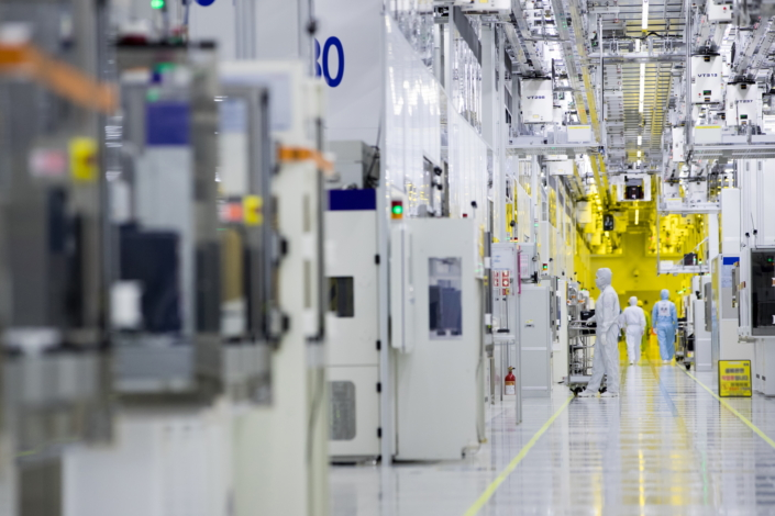
The project’s total price tag is expected to exceed $40 billion. In Taylor, Samsung plans to build three fabs and a chip packaging plant. The company will also use a portion of the financing to upgrade its existing semiconductor facilities in nearby Austin.
“I signed the CHIPS and Science Act to restore U.S. leadership in semiconductor manufacturing and ensure America’s consumers, businesses, and military maintain access to the chips that underpin our modern technology,” said President Joe Biden. “This announcement will unleash over $40 billion in investment from Samsung, and cement central Texas’s role as a state-of-the-art semiconductor ecosystem.”
The main highlight of the project is a pair of new fabs in Taylor that will make processors based on two- and four-nanometer manufacturing technologies. Samsung’s four-nanometer node entered mass production in 2021. Its two-nanometer technology, in turn, is expected to roll out next year.
The first two-nanometer chips Samsung plans to make will reportedly be geared toward mobile devices. In 2026, the company intends to roll out an enhanced version of the node to make chips for high-performance computing environments such as cloud data centers. A year later, Samsung will start making two-nanometer processors for vehicles.
Alongside the two processor plants, the Taylor complex is set to host a research and development fab. It will support Samsung’s efforts to enhance its manufacturing processes, a push that will eventually see the company move beyond two-nanometer technologies.
Samsung is expected to roll out a so-called 1.4-nanometer process in 2027. The technology will reportedly feature an enhanced version of the gate-all-around, or GAA, transistor design that underpins the company’s latest chips.
Transistors leverage a mechanism known as a channel to move electricity between their internal components. In Samsung’s GAA design, the channel is implemented as three nanosheets stacked atop one another. The company’s 1.4-nanometer process will reportedly boost the number of nanosheets in each transistor to four, which is expected to increase performance and reduce power usage.
The three fabs in Taylor will operate alongside a facility dedicated to producing 2.5D packaging components. Those are parts used to link together multiple semiconductor modules into a single product. Nvidia Corp., for example, uses packaging to link together its graphic cards’ onboard compute and memory modules.
The 2.5D packaging that Samsung’s planned facility will produce links together semiconductor modules by placing them side-by-side on a shared base layer. This base layer, or interposer, includes tiny wires that allow data to move between the modules installed on top. Some types of interposers also include networking circuits that help speed up the movement of data.
As part of the investment announced today, Samsung also plans to upgrade its existing semiconductor facilities in Austin. The effort will focus on enhancing the company’s ability to make chips based on so-called FD-SOI technology.
In a FDO-SOI chip, transistors are implemented as a layer of insulating material sandwiched between two layers of silicon. Such transistors can manipulate electricity more efficiently than circuits based on designs such as the GAA architecture. Additionally, they use less power and are simpler to produce.
FDO-SOI technology is widely used to make wireless networking chips, as well as certain other circuits that must operate with a high degree of power efficiency. The Commerce Department said that Samsung’s FDO-SOI facilities in Austin will make chips for critical U.S. industries such as the aerospace, defense and auto sectors. The company has reportedly made a “series of commitments” to produce chips for the U.S. Defense Department at the Austin site.
Across all the facilities Samsung intends to build or upgrade, the investment is expected to create 21,500 jobs. The company will spend $40 million of the federal funding it has won today on workforce development initiatives such as training programs.
The financing will be provided through the 2022 CHIPS and Science Act, which allocates $39 billion in direct grants for the chip sector along with $75 billion worth of loans and loan guarantees. Intel Corp., Taiwan Semiconductor Manufacturing Co. Ltd. and several other market players have also received federal financing recently to expand their chip infrastructure in the U.S.
THANK YOU